Active Circuit Design -Final Report
Active Circuit Design -Final Report
Power Amplifier Design using HBT Technology
—implement a 2.4GHz Power amplifier MMIC for IEEE.802.11.b/g
Student Name: Lan, Wen-Chun (Randall) 藍文鈞
June 22nd, 2016
Abstract
Wireless communication is being part of your life. It provides seamless service where you are. 2.4 GHz frequency band is widely used in data communication system in the ISM band. For example, it is used in Wi-Fi IEEE 802.11.b/g/n/ac, Bluetooth, UWB, Zigbee applications and etc.
In this paper, we use 2.0um HBT technology of Win Semiconductor Company to implement a 2.4Ghz Power Amplifier (PA) MMIC. The 2.4 GHz PA MMIC is manufactured on Gallium Arsenide Heterojunction Bipolar Transistor (GaAs HBT) process. The device is a low cost, high linearity, medium power, high efficiency amplifier IC, designed for IEEE 802.11b/g, Bluetooth Class 1, and other applications in the 2.4GHz ISM band.
The device features analog power control to optimize transmitting power while maximizing battery life in portable equipment. The device includes an integrated current mirror to support stable out power and power detector circuit for closed loop control of output power.
The PA MMIC can be packaged in a compact 3mm by 3mm QFN-12L package with a backside ground and thermal release function.
Key Words: ISM Band, Bluetooth, UWB, Zigbee, HBT technology, GaAs, Current mirror, power detector.
- Introduction
The 2.4 GHz PA MMIC is manufactured on Gallium Arsenide Heterojunction Bipolar Transistor (GaAs HBT) process. The device is a low cost, high linearity, medium power, high efficiency amplifier IC designed for IEEE 802.11b/g, Bluetooth Class 1, and other applications in the 2.4GHz ISM band. The device also features analog power control to optimize transmit power while maximizing battery life in portable equipment. The device includes an integrated power detector circuit for closed loop control of output power. For getting stable output power, a current mirror circuit is built on the 2nd stages bias circuit. The PA MMIC is packaged in a compact 3mm by 3mm QFN-12L package with a backside ground.
In this MMIC, there are 2 stages power amplifier integrated together. In the 1st stage, the transistors contribute 18 dB Gain as a driver stage, and 2nd stage is the power stage, which contributes 6 dB gain and 24dBm power out. The total conversion gain is 24 dB and provides +23 dBm at power one dB compression point. In Fig 1, the block diagram shows the function blocks. There are 2 stages in the MMIC. The power detector can be used as DC level proportional to power output, which can be used in close loop power control to get fixed power out.
The Vcc2 is the Power out pin as well as the bias of 2nd stage. They are output pins with low output impedance to get high power out. PD is the Vb1 of the 1st stage and APC is the Vb2 of the 2nd stage to control the gain and power out, which can be controlled by analogy signal. There are 2 GND pins to protect the RF in for reducing the noise interference and being the part of input matching.
There are 12 pins on the QFN package, but for smaller design, the MMIC can be built in DFN-8L-2x2mm and the RF performance will be better. But the thermal effect will be poorer than 3x3mm.
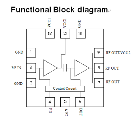
Fig 1, the MMIC function block diagram shows 2 stages PA with power detector and control pins.
In the Fig 2, it is the layout of the MMIC. There are two GND via-through to the Bottom side. The thickness of the die is 4 mil for shorten the via length to get smaller the inductor and resistor. The inductor and resistor series to Emitter of transistor affect the Gain and power out very much.
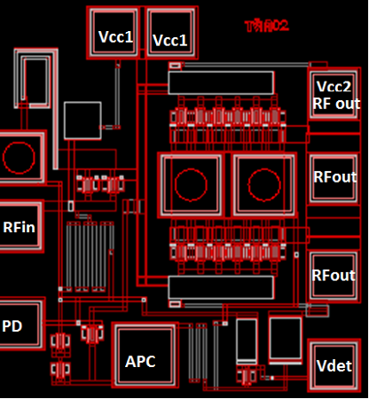
Fig 2, the MMIC layout and pin names, with dimension 700um x 900um
- Design consideration and simulation
In the circuit design, we have some features and targets:
- Stable output power, no overshooting while load changing
- Power detect out
- Gain control
- Power control
- 24 dB gain with <22+ dBm power out
- Linear power out +19 dBm based at +3.3V and meet APCR requirements.
In Fig 3, the circuit is the complete simulation circuit using Agilent ADS system. The scalable transistors models were created by author’s team based on lots of testing. The 1st stage contributes 18 dB and 2nd stage contributes 6 dB biased at +3.3V.
Fig 3, the PA MMIC circuit and simulation template using Agilent ADS
The transistors are designed and fabricated by foundry. A designer cannot do any better, but designer can design unique, stable DC bias circuit and get a good MMIC with excellent performance.
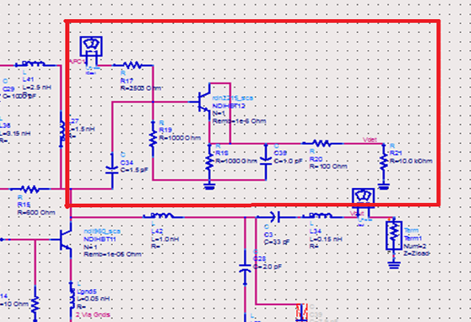
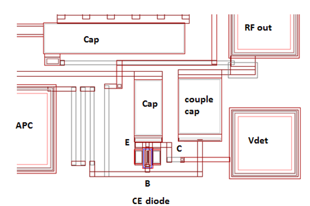
Fig 4, the Vdet circuit and layout
In Fig 4, we use C14 to couple power out from the Collector of last stage of PA and a CE diode to detect the voltage level which is proportional to the output power. A capacitor is used to filter out the high frequency signal and a Resistor to adjust the DC level.
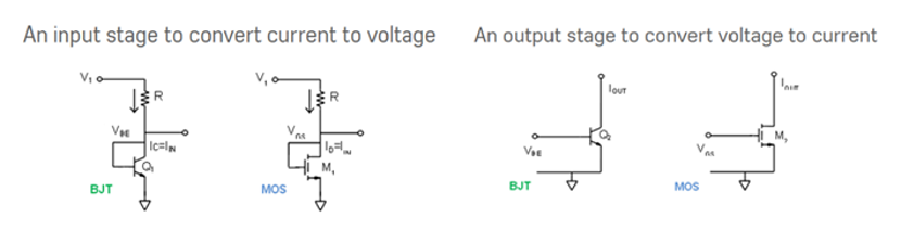
Fig 5, Current Mirror
A current mirror circuit is designed in the bias circuit for the PA. It provides high isolation to get stable power out under continuously load change. The input stage converts current to voltage and output stage converts voltage to current. The circuit provides a stable current source for the last stage of the PA MMIC.
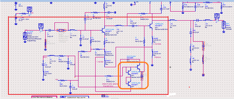
Fig 6, current mirror circuit is used in the DC bias of the MMIC
In Fig 4, it shows the current mirror circuit. Its function is providing a stable Ib2 to 2nd stage of the PA. And the circuit is biased by Vpd. It means 2nd stage is turn on after 1st stage turn on always. Its sequence is listed as below:
- Vpd on, the 1st stage Vb1 is setup. The 1stage is turn on.
- And Vpd is the Vcc of Current mirror for the 2nd stage. Vapc is on and build up a Vb2 (more than +2.6V) for the current mirror. Then, 2nd stage is turn on.
- The sequence is Vpd on, 1st stage on, Vapc on, 2nd stage on.
The sequence make sure that the PA is turn on step by step and without over shorting. Its spectrum response will be under regulation limits and meet FCC requirements.
Simulation results
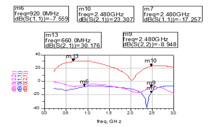
Fig 7, the plot shows S11, S21 and SS of the simulated PA circuit
In the Fig 6, it shows S21 has good performance at 900MHz. The original idea is we can design out a dual band PA MIIC used in 2.4 GHz and 900 MHZ in ISM band. But in harmonics and spurious limitation, it is not accepted.
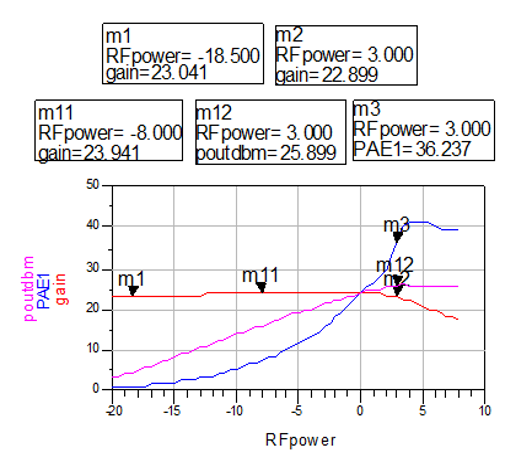
Fig 8, it shows the power out, Gain and PAE of the PA
In Fig 7, the plot shows the Power 1 dB compression is at 25.899 dBm and its PAE is 36.237%. And it has 23.941 dB Gain. It meets our targets.
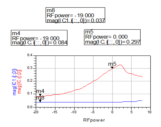
Fig 9, it shows the total current consumption will be 297mA when Pin is 0dBm.
In Fig 8, the power out is 23dBm and current consumption is 297mA while Pin is 0 dBm.
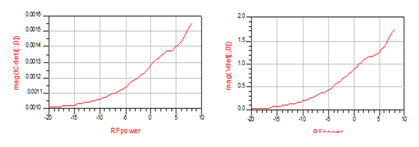
Fig 10, it shows the Vdet level and Idet vs Pin
In Fig 9, the Vdet level can be adjusted by pull up resistor before output. The reasonable output level will be 1V~3V vs 10dBm~25dBm.
- Circuit Layout
The HBT process flow is from Foundry Company. Before starting to do layout, you need to be familiar with the whole process flow. It can help you to know the layers of mask. There are 18 steps in the process. In the Fig 11, it shows the flow of HBT process. There are 2 optional steps. The minima required layers of mask are 16 layers. In Fig 11, it is a 3D structure of the process, which shows capacitor, resistor, Schottky diode and transistor of HBT with colors assignment. The colors assignment can help designer to recognize layers of mask. We suggest designers to follow the colors assign for layers.
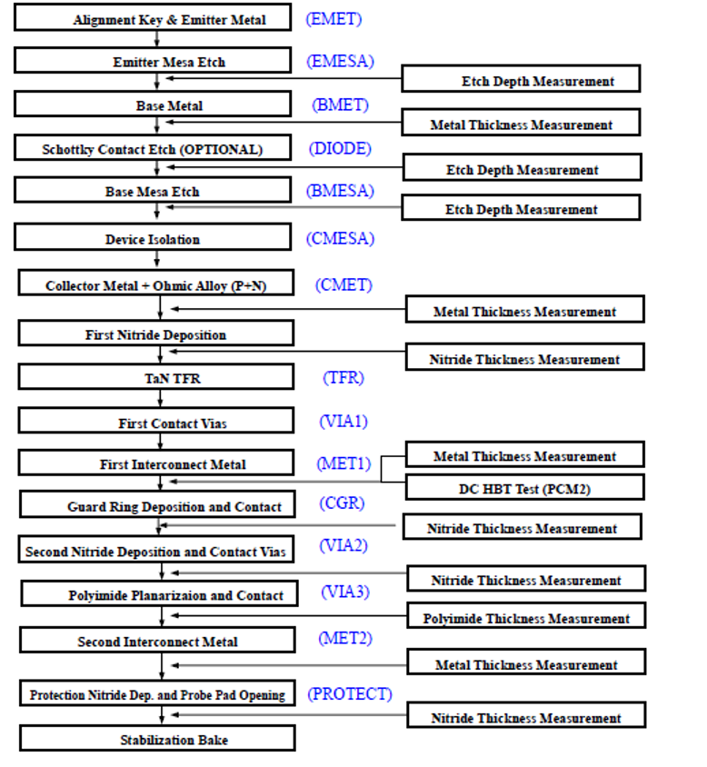
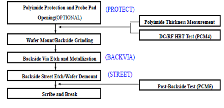
Fig 11, HBT process flow
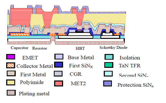
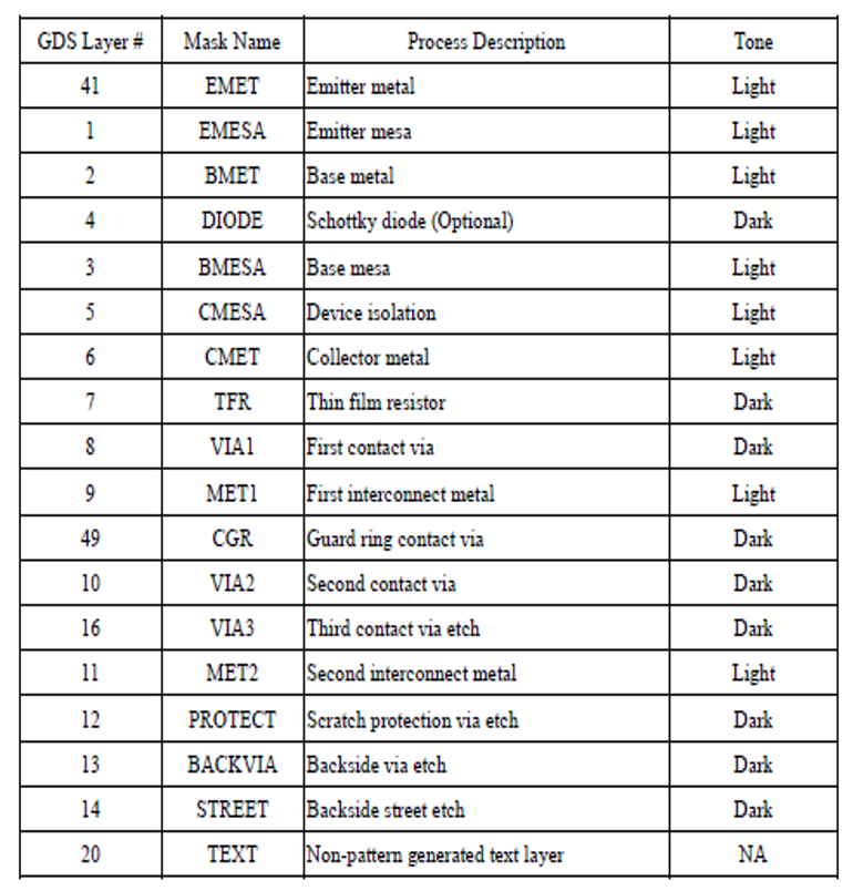
Fig 12, the HBT Mask layers name and 3D structure with Color assignment
In Fig 13, it shows the standard cell from foundry. It has 2 emitter fingers which is 2um width and 20um length. It supports 20mA current consumption and 60mW max. The parameters table shows the cell name, which is the model of design kit.
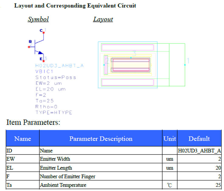
Fig 13, a transistor layout and design rule
In Fig 14, it shows diode, resistor and stack capacitor standard cell and shows the resistor, which layer is TFR, design rule and limitations.
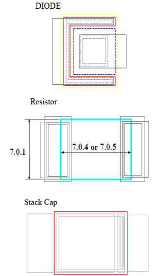
Fig 14, the standard cell and design rule of HBT process for doing layout design
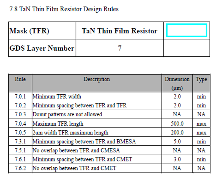
Fig 15, a layout rule example: the resistor design rule of HBT process for doing layout design
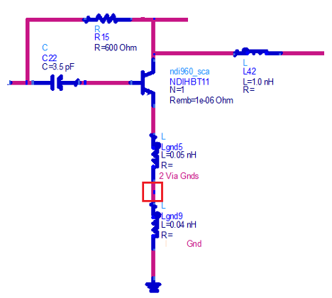
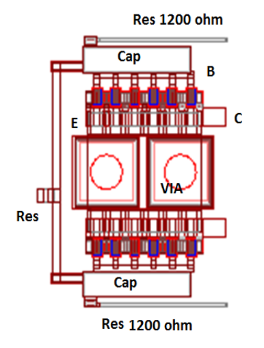
Fig 16, the 2nd stage of PA MMIC, its transistor size is 960um
In Fig 16, it is the 2nd stage of MMIC, which size is 960um (2 x 2 um x 20 um x12), which can be driven up to 25dBm with 6 dB gain. In the simulation circuit, there are an inductor and a resistor added to simulate via-thru. There are two 1200 ohms resistors paralleled to be 600 ohms connected to Collector of the PA as a feedback path. And there are two capacitors shunted together to be 3.5pF connected to Base of the transistors.
In Fig 17, the circuit of 1st stage of PA shows the transistor size 2 x 2um x15um x N (is the scalable factor). The transistor model is scalable. In Fig 17, the 1st stage transistors show the size 2 x 2um x 15um x 2 (N), which provide 18 dB gain and 18 dBm power out. It s Base is biased by Vpd, which controls the gain of 1st stage of the PA.
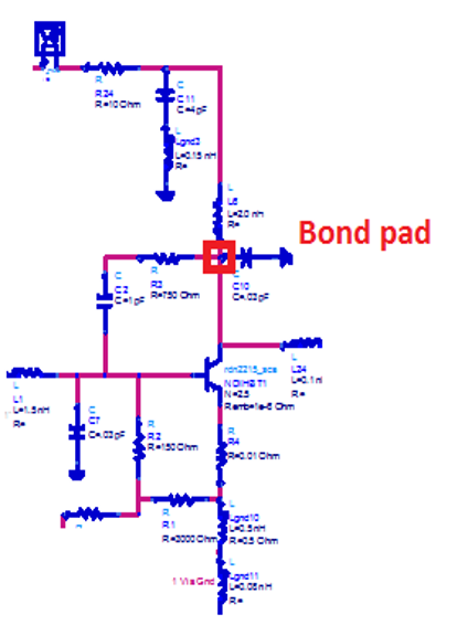
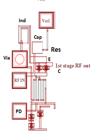
Fig 17, the circuit of 1st stage, which shows the transistor size 2x 2um x15um x 2 pcs with scalable factor N
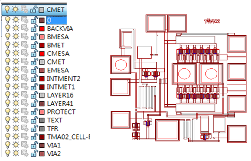
Fig 18, the complete PA MMIC layout with layers assignment table
Post Simulation
There are some chances as below that you need to change the distributed capacitors, inductors and resistors:
- The traces length change continuously while changing the location of capacitors, transistors, and resistors.
- Via-thru of substrate is molded as inductor and resistor.
- Modeling of multi-bonding wires.
- Modeling of bonding pads.
It is for sure that the model of inductor is accurate from Foundry Company. But we need to use different Inductor value and different layout. The Modeling Inductors using HFSS 3D is a good way to create the S-parameters as a two ports network.
- Final test results
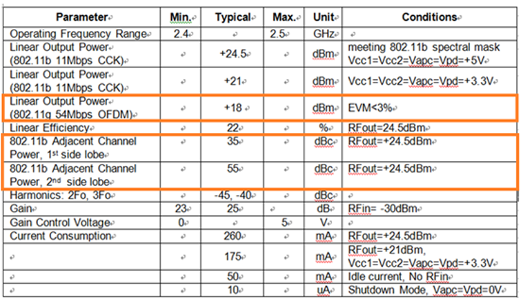
The table 1 shows the measured data for IEEE 802.11.b/g. The PA is working at Class A as a linear power amplifier.
Table 1, For IEEE 802.11.b/g applications
In the Table 2, it shows the measured data for Bluetooth class I. The PA is working in Class AB, which ideal efficiency will be 78%. And we get 40% at P-1dB point. It is a good design comparing with simulation results.
Table 2, For Bluetooth class 1 application
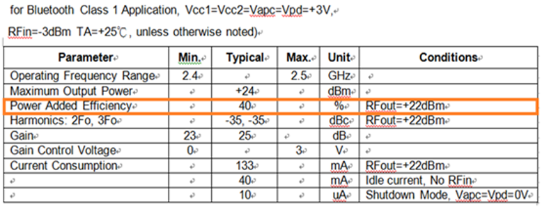
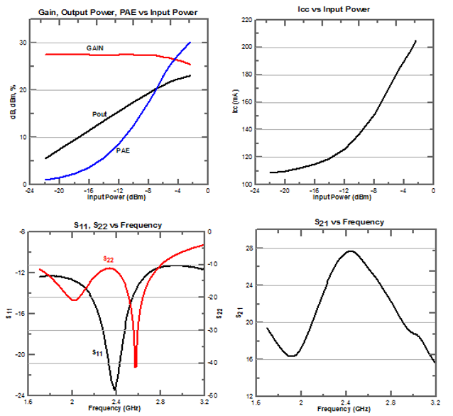
Fig 19, the measured data of the PA MMIC packaged in QFN-3x3mm-12L
- Conclusion
The 2.4 GHz Power Amplifier MMIC using 2.0um HBT technology is successfully implemented in 700 x900um dimension. There are 2 stages to contribute 24 dB gain with 25 dBm power out in the MMIC. It is good for IEEE 802.11.b and g, and Bluetooth, Zigbee, UWB and other portable data terminals.
We use current mirror circuit to get stable power out and get more reliable PA life. It provides a good isolation between changing loads and output stage of the PA. A power down control pin is implemented as well for control the gain stage. The APC and PD contribute getting good control of gain, power and PAE.
The PA MMIC is built in QFN-3x3mm-12L, not just for low cost and good thermal and RF performance. But also It provides outstanding compete capability in the market.
For the newer and more complex modulation technologies developing, the linear PA MMIC is required urgently. For example: IEEE 802.11.n/ac or IEEE 802.11.x, the market needs supper linear PA with 2% EVM. And the design and process will be more difficult in the near future.
Reference
- ADS Version 2012
- Jacob Millman and Arvin Grabel3, Microelectronics Sedra/Smith , Microelectronics circuits, version
- S.S. Rajput, S.S. Jamuar, A Current Mirror for Low Voltage, High Performance Analog Circuits, Analog Integrated Circuits and Signal Processing, September 2003, Volume 36, Issue 3, pp 221-233
- Win Semiconductor Company design kit